VLSI Design Categories
Analog VLSI
Analog VLSI Design
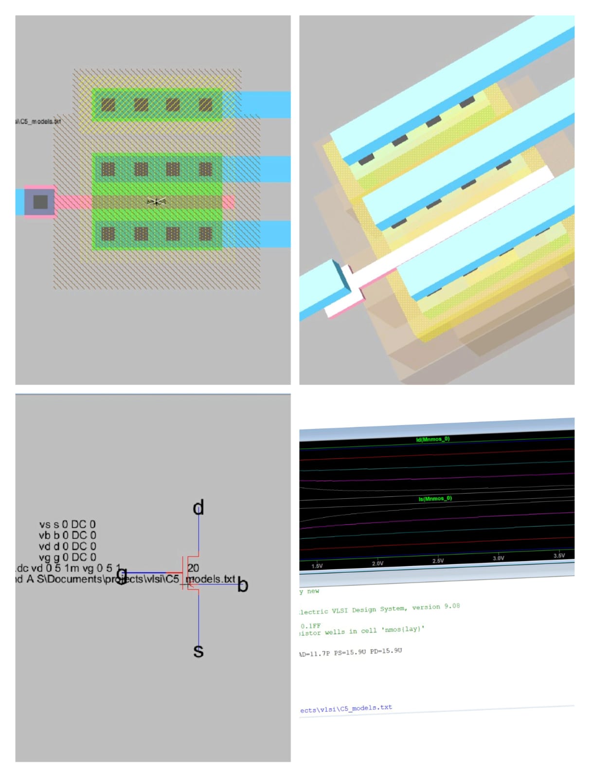
Composite view: Layout, Schematic, 3D model, and Simulation
NMOS Transistor Layout (Electric VLSI)
2025 | Completed (Foundational Project)
A foundational VLSI project designing a single NMOS transistor from schematic to physical layout. This project served as an introduction to the VLSI design flow, tools, and fundamental concepts of layout using the Electric VLSI EDA tool and C5 process technology files.
Key Features & Parameters:
- Device: NMOS Transistor
- Channel Width (W): 6μm
- Channel Length (L): 0.6μm
- Technology: C5 Process (0.6μm)
Design Methodology:
Tools & Technologies:
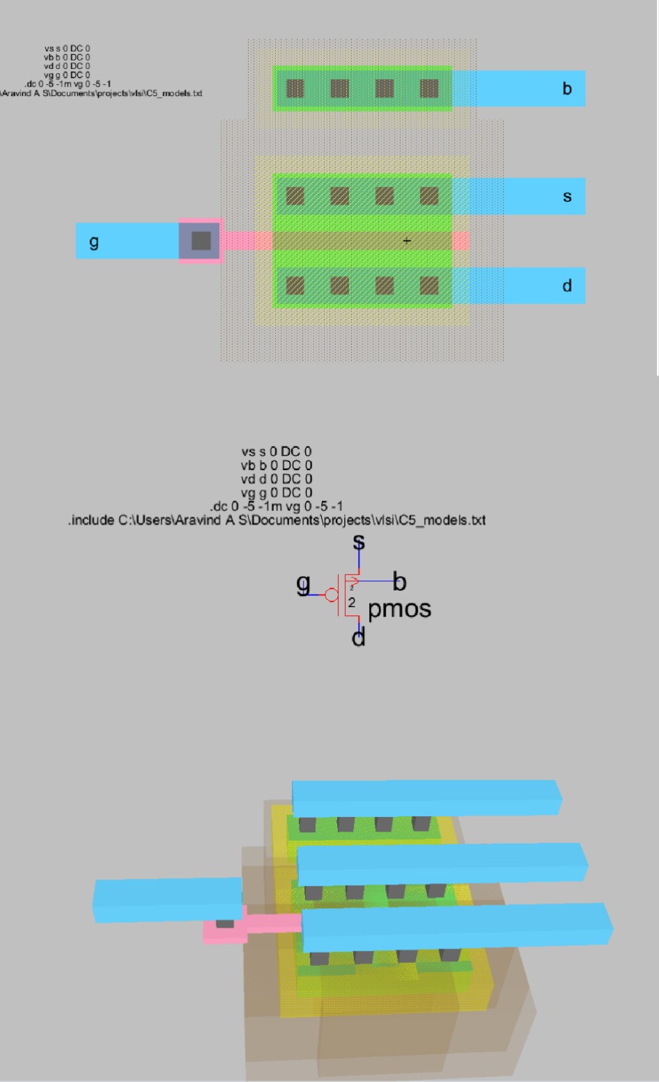
Composite view: Layout, Schematic, and 3D model
PMOS Transistor Layout (Electric VLSI)
2025 | Completed (Foundational Project)
A foundational VLSI project designing a single PMOS transistor from schematic to physical layout. This project served as an introduction to the VLSI design flow, tools, and fundamental concepts of layout using the Electric VLSI EDA tool and mcmos 300 technology files.
Key Features & Parameters:
- Device: PMOS Transistor
- Channel Width (W): 6μm
- Channel Length (L): 0.6μm
- Technology: mcmos 300
Design Methodology:
Tools & Technologies:
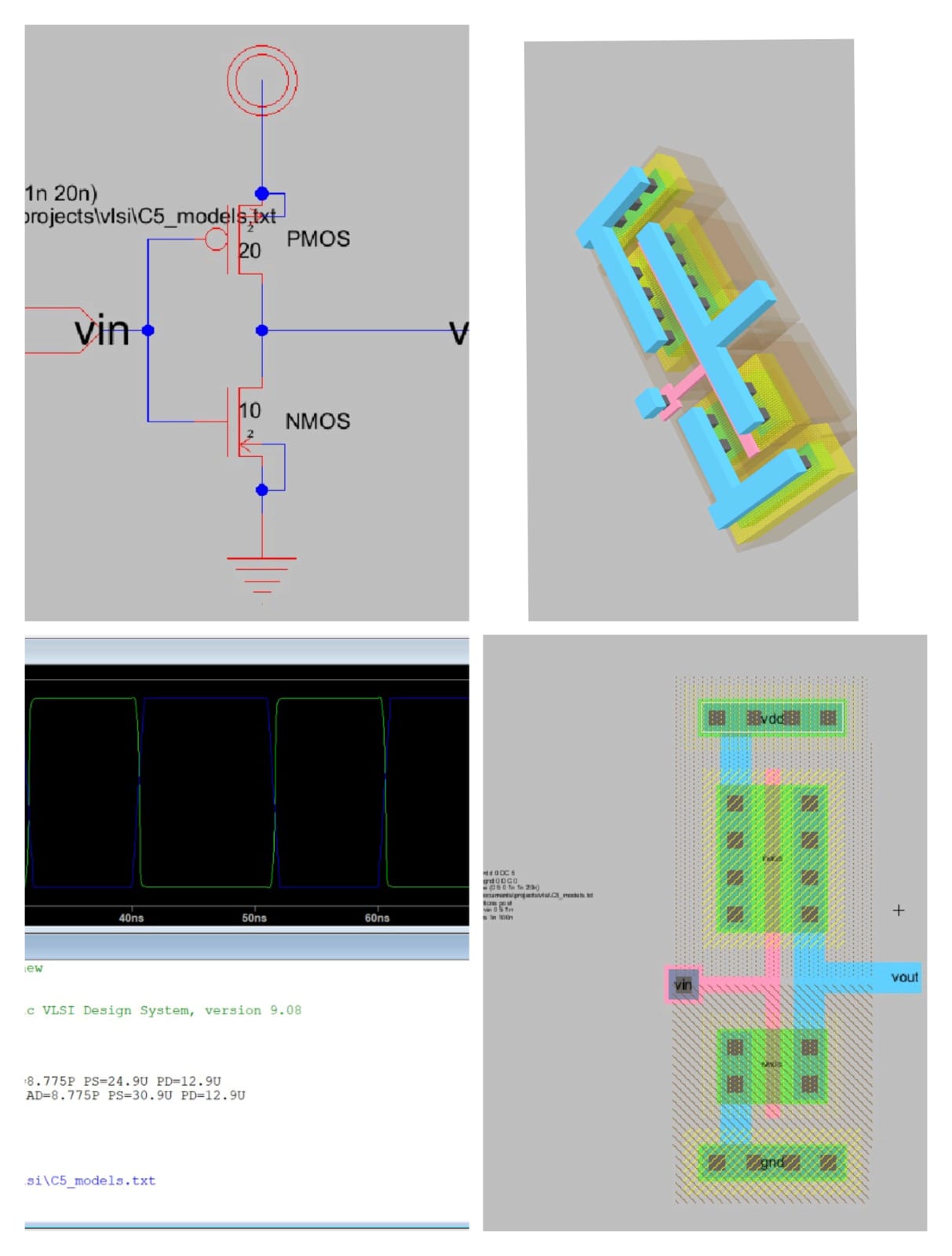
Composite view: Schematic, Layout, 3D model, and Simulation
CMOS Inverter Layout (Electric VLSI)
2025 | Completed (Foundational Project)
A fundamental digital logic gate, the CMOS inverter, designed from schematic to physical layout. This project demonstrates the core principles of matching PMOS and NMOS transistors and verifying the design's transient (inverting) response using the Electric VLSI EDA tool.
Key Features & Parameters:
- Device: CMOS Inverter
- PMOS (W/L): 6μm / 0.6μm
- NMOS (W/L): 3μm / 0.6μm
- Technology: mcmos
Design Methodology:
Tools & Technologies:

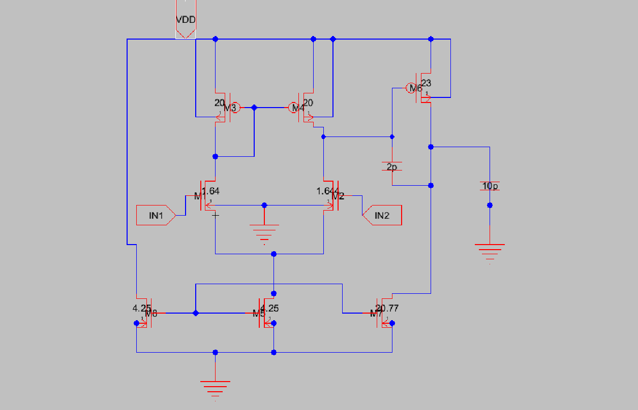
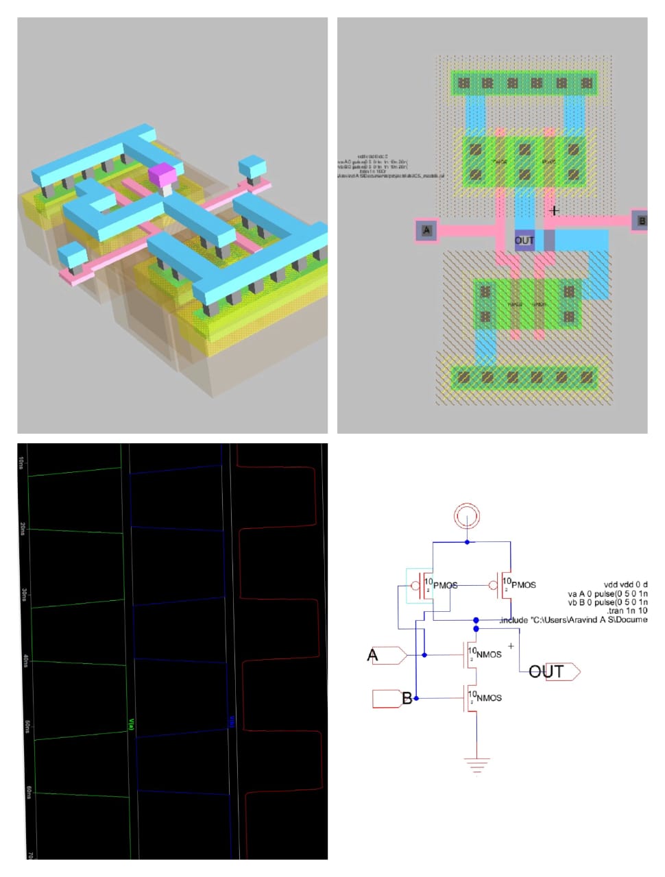
Circuit Schematic
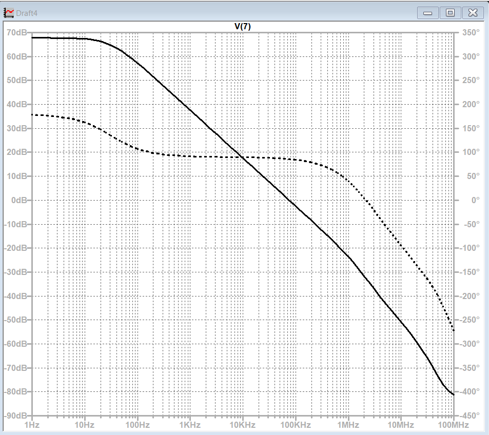
AC Simulation (68dB Gain)
Ultra-Low Power Biomedical Op-Amp (VLSI)
2025 | Completed (LIC Course Project)
A two-stage CMOS operational amplifier designed from transistor-level for biomedical wearable devices. The core challenge was achieving ultra-low power consumption (nano-ampere range) while maintaining high gain and stability, suitable for amplifying weak biosignals like ECG or GSR.
Key Features & Results:
- Ultra-Low Power: ~1.7 $\mu$W consumption
- DC Gain: ~68 dB
- Bandwidth: 100 kHz Gain-Bandwidth Product
- Highly Stable: 90° Phase Margin
- Technology: 1$\mu$m CMOS (Subthreshold)
Design Methodology:
Tools & Technologies:
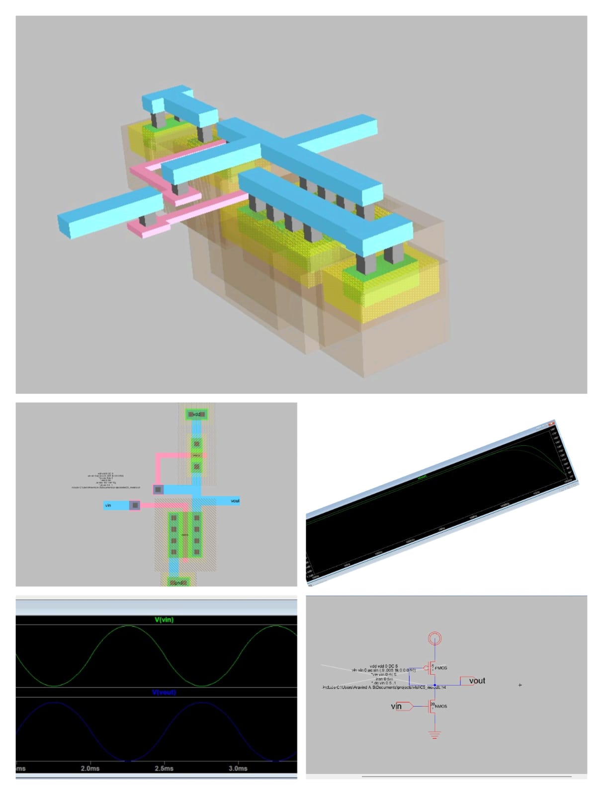
Composite view: 3D Layout, Layout View, and Transient Response
Common Source Amplifier (Diode-Connected Load)
2025 | Completed
Designed and simulated a Common Source (CS) amplifier using a diode-connected PMOS transistor as an active load. This topology replaces the passive resistor to save chip area and provide a non-linear resistance, demonstrating fundamental analog IC design principles.
Key Features & Parameters:
- Driver (NMOS): W = 20μm, L = 2μm
- Active Load (PMOS): W = 5μm, L = 2μm
- Topology: Diode-Connected Load
- Analysis: DC Operating Point & Transient
Design Methodology:
Tools & Technologies:
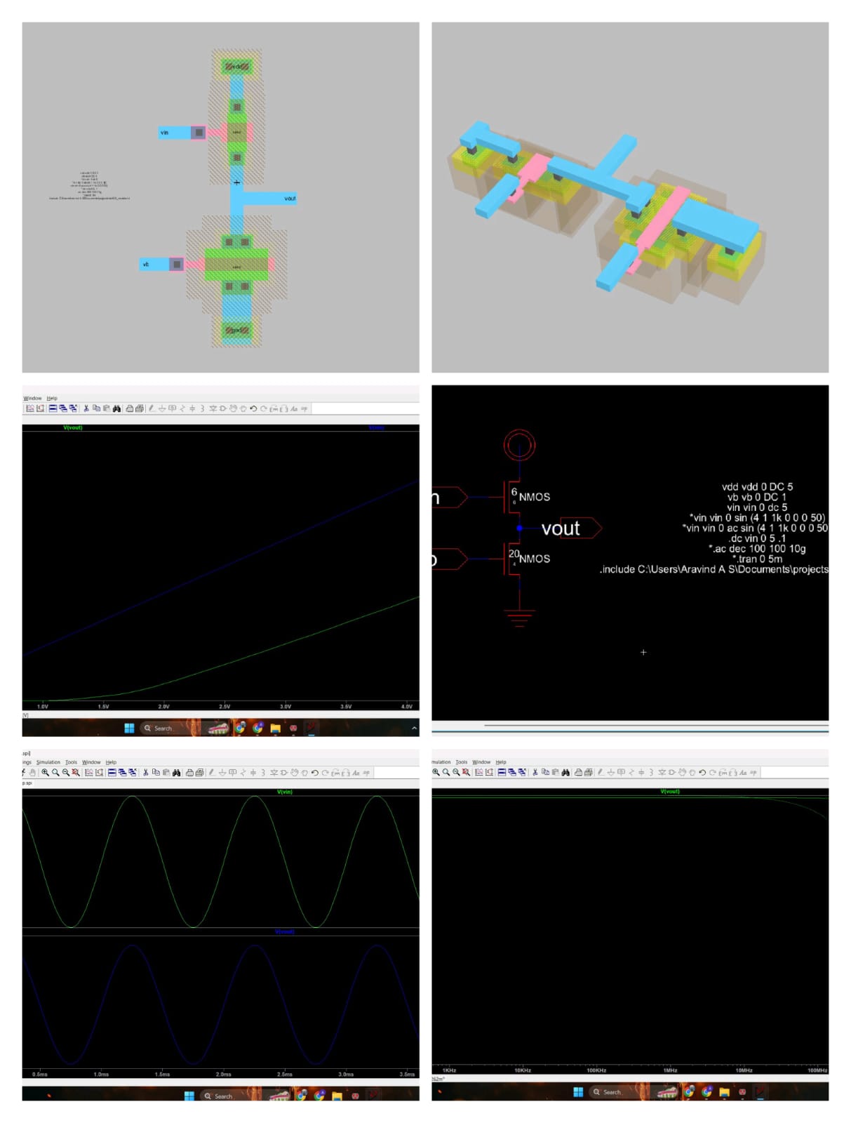
Composite view: Layout, 3D Model, Schematic, and Simulation
Common Drain Amplifier (Source Follower)
2025 | Completed
Designed and simulated a Common Drain (CD) amplifier, also known as a Source Follower, using NMOS transistors. This topology acts as a voltage buffer with unity gain ($A_v \approx 1$), high input impedance, and low output impedance, making it ideal for driving low-resistance loads or serving as an isolation stage.
Key Features & Parameters:
- Driver NMOS (Top): W = 6μm, L = 6μm
- Load NMOS (Bottom): W = 20μm, L = 4μm
- Topology: Source Follower (Active Load)
- Gain: ~1 V/V (Voltage Buffer)
Design Methodology:
Tools & Technologies:
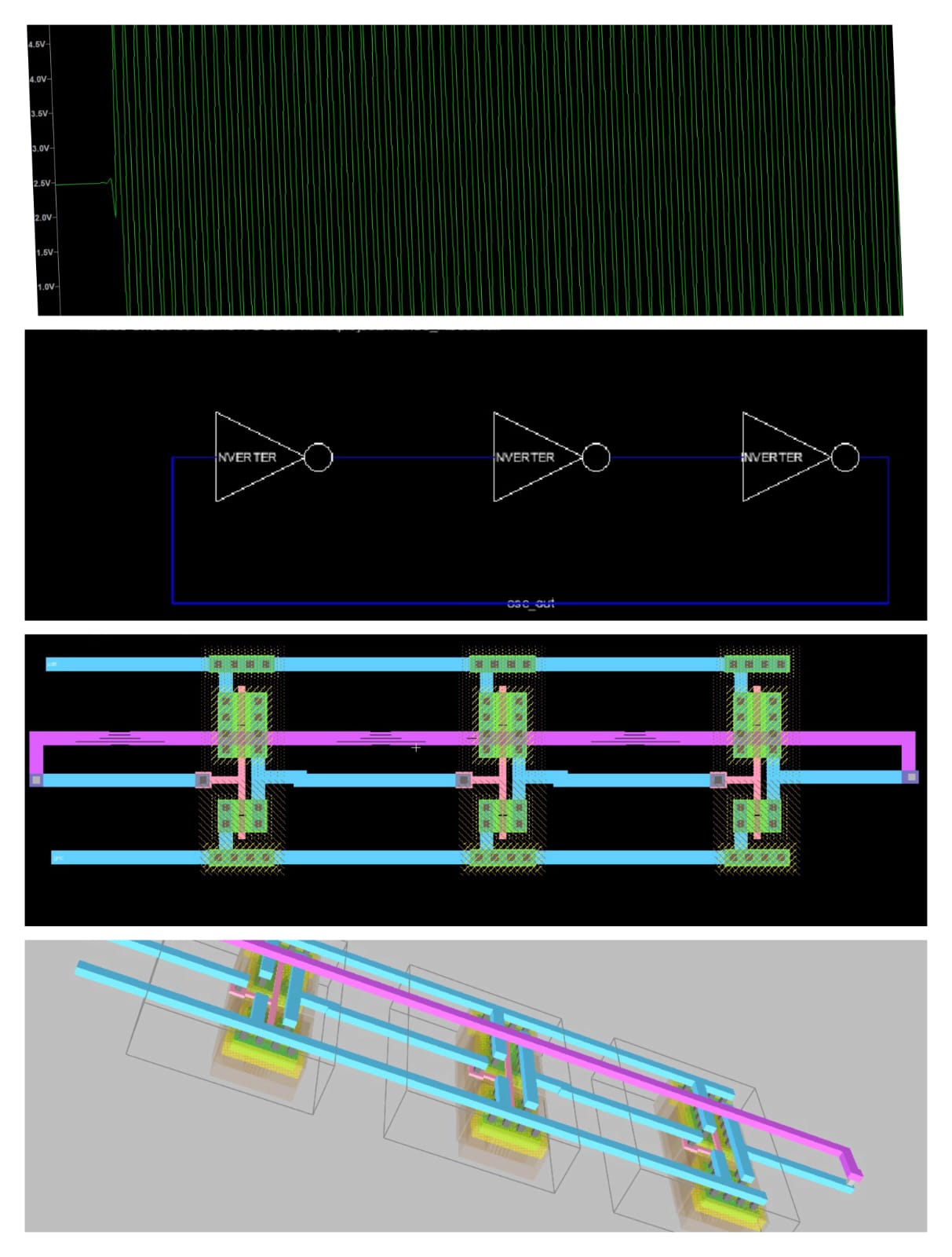
Composite view: Transient Simulation, Schematic, Layout, and 3D View
Three Stage Ring Oscillator (Electric VLSI)
2025 | Completed
Designed and simulated a 3-stage Ring Oscillator by converting the previously designed CMOS Inverter into a reusable schematic symbol. The project involved connecting three inverters in a feedback loop to generate self-sustaining oscillations and designing the compact physical layout.
Key Features & Parameters:
- Topology: 3-Stage Feedback Loop
- Methodology: Symbol Creation & Instantiation
- Output: Self-Sustaining Oscillation
- Layout: Cascaded CMOS Inverters
Design Methodology:
Tools & Technologies:
Composite view: 3D Layout, 2D Layout, Transient Response, and Schematic
CMOS NAND Gate Layout & Simulation
2025 | Completed
Designed and verified a 2-input CMOS NAND gate from transistor-level schematic to physical layout. This project demonstrates the implementation of universal logic gates using complementary MOS technology, ensuring balanced switching characteristics through precise transistor sizing.
Key Features & Parameters:
- Universal Logic: Transistor-level implementation of NAND function.
- Architecture: Parallel PMOS pull-up and series NMOS pull-down networks.
- Technology: Designed using Electric VLSI with the C5/mcmos process.
- Verification: Confirmed via DRC, LVS, and transient SPICE simulation.
Design Methodology:
Tools & Technologies:
Digital VLSI Design (FPGA)
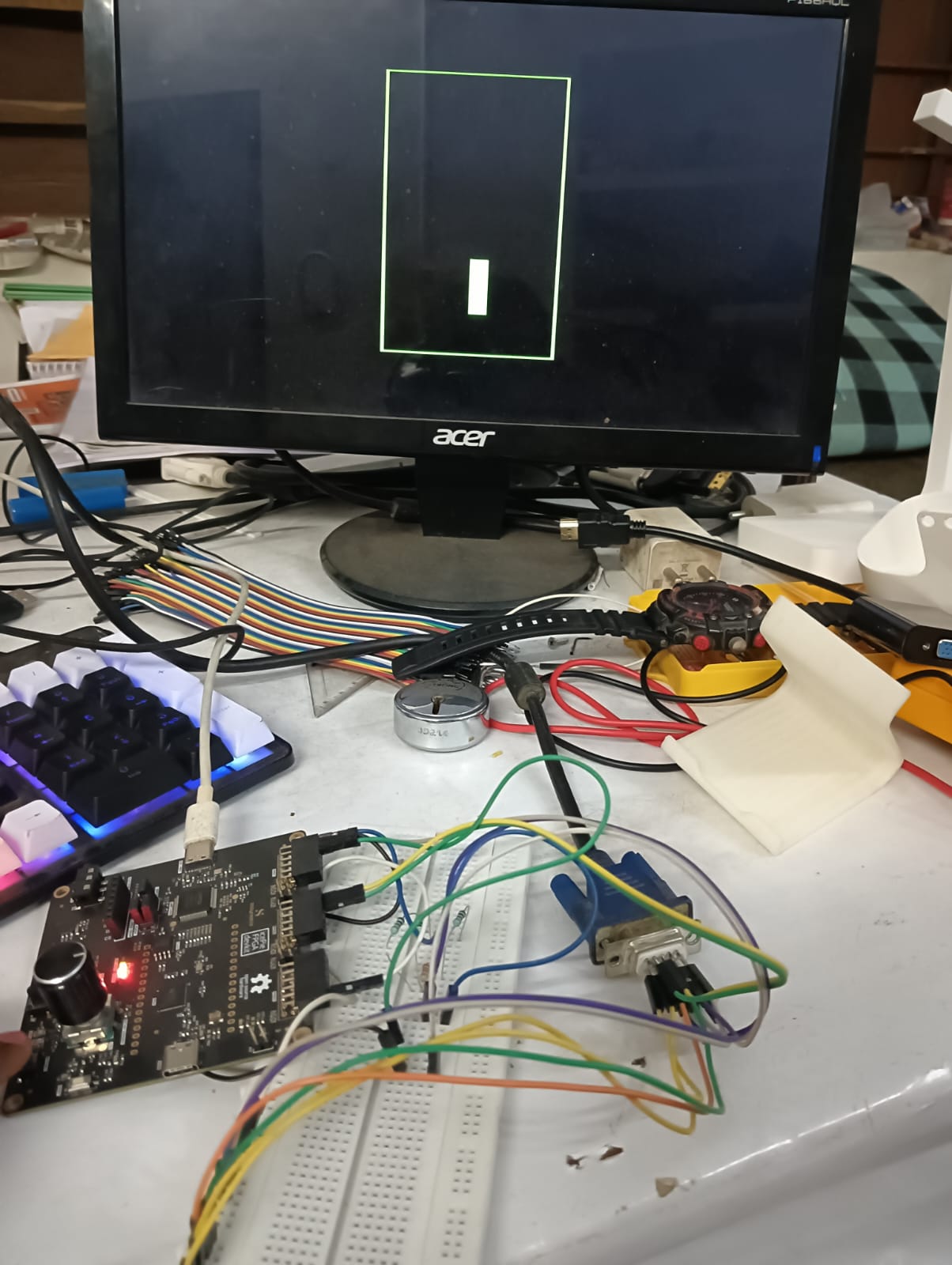
Pong with Scoreboard on FPGA using VGA
2026 | Completed
This project implements a classic Pong arcade game on an iCE40 FPGA, displayed on a VGA monitor, with an enhanced real-time scoreboard system. The game features player-vs-AI logic, where the left paddle is controlled by physical buttons and the right paddle is driven by a simple AI. Background music is played through a speaker output throughout the game.
Key Features:
- VGA 640×480 @ 60Hz display using custom timing logic
- Two-digit score display using a hardware 7-segment-style pixel renderer
- AI-controlled opponent as a 3-state Moore FSM
- Background music playback using a note-sequencing FSM
- Virtual win/loss detection via background color change
Technical Implementation:
Technologies Used:
Building Tetris on FPGA using VGA 🎮⚡
2026 | In Progress
Currently working on implementing a classic Tetris game using FPGA with VGA output, combining digital design, debugging, and real-time graphics. Currently in the debugging phase, optimizing display timing, block rendering, and control logic.
What I’m exploring:
- VGA signal generation (HSYNC, VSYNC, pixel timing)
- Game logic implementation in Verilog
- Real-time rendering of blocks on screen
- Hardware debugging and timing optimization
Technologies Used:
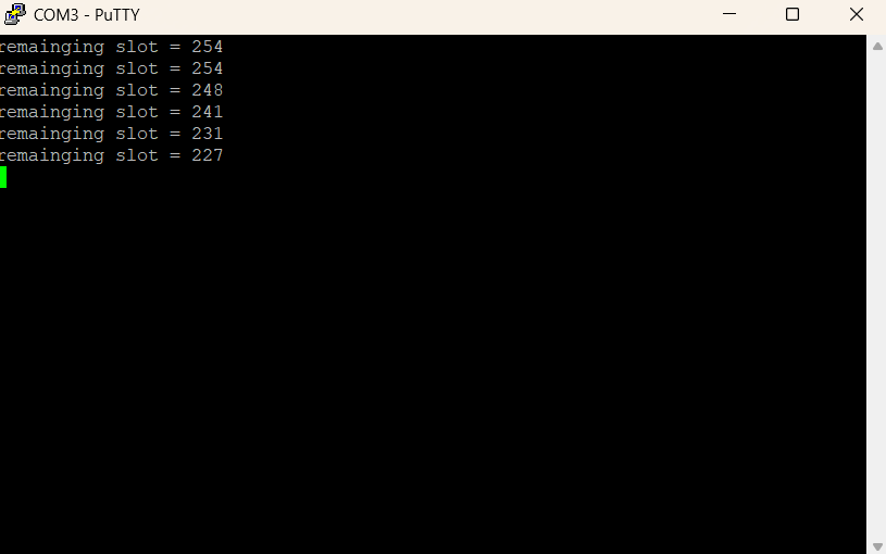
Car Parking Slot Using FPGA
2025 | Completed
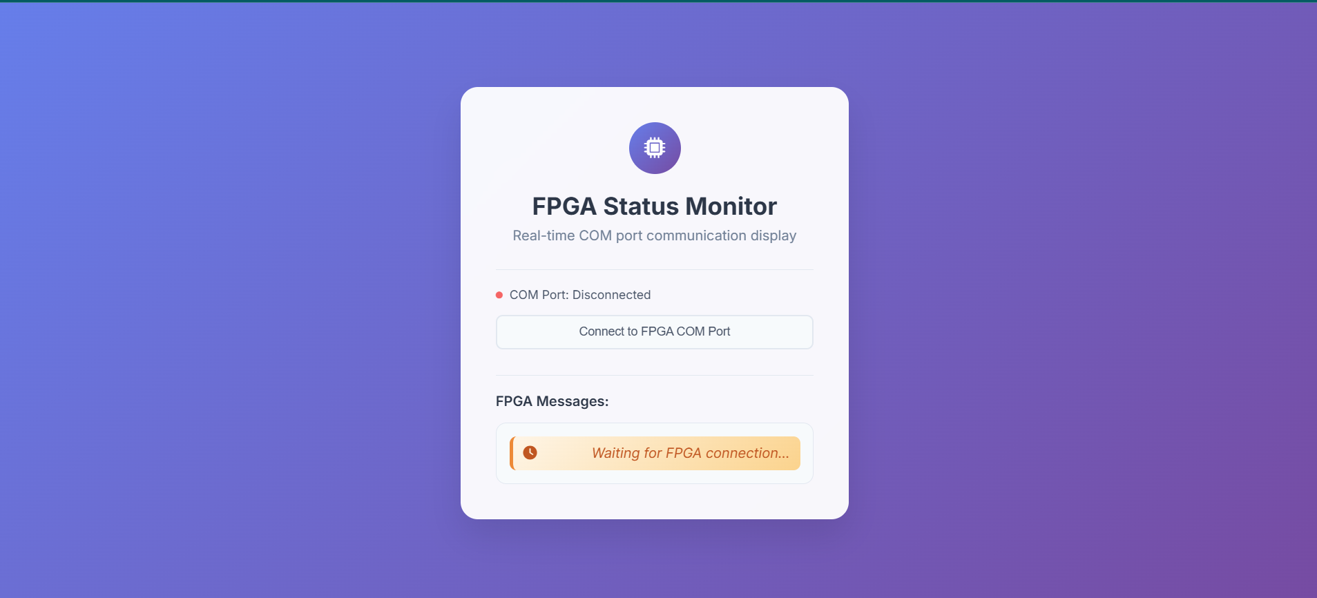
A Verilog-based parking slot counter system implemented on the iCEPi FPGA board. The design uses two push buttons — one for incrementing (car entry) and another for decrementing (car exit). The counter ranges from 0 to 255 (8-bit), simulating parking slot availability. Real-time count data is sent via UART (9600 bps) to a Python + HTML web interface for live display.
Key Features:
- Increment counter for car entry
- Decrement counter for car exit
- 8-bit counter (0-255 range)
- UART communication at 9600 bps
- Python + HTML web interface for display
Technical Implementation:
Tools Used:
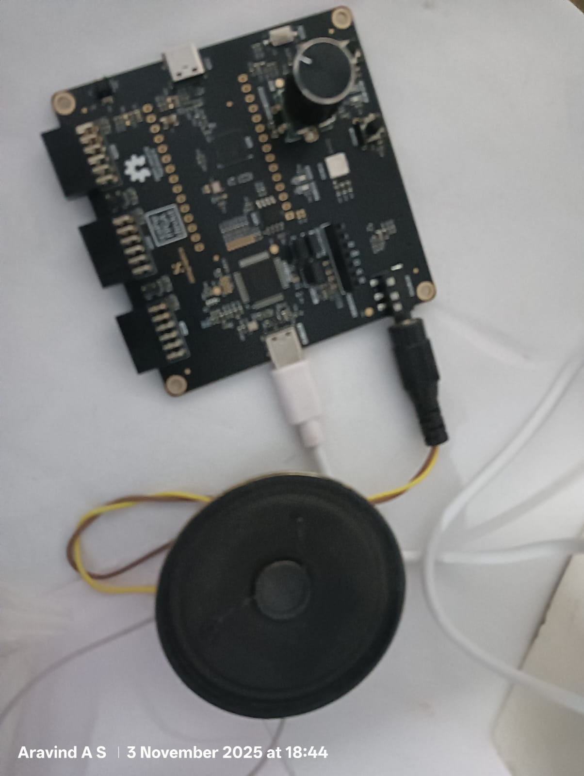
FPGA-Based Music Instrument using One Rotary Encoder
2025 | Completed
A digital music synthesizer built in Verilog on the iCEPi FPGA board. A single rotary encoder controls tone frequency and waveform selection. The generated audio is output through AUX to a speaker, while note information is sent via UART (9600 bps) to a Python + HTML web interface for real-time visualization.
Key Features:
- Single rotary encoder controls tone frequency and waveform selection
- Audio output through AUX to speaker
- UART transmission of note information at 9600 bps
- Real-time visualization via Python + HTML web interface
Technical Implementation:
Tools Used:
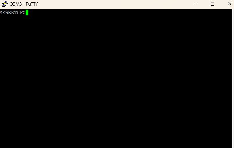
Morse Code Encoder/Decoder (FPGA)
2025 | Completed
A Verilog-based Morse Code Encoder and Decoder implemented on FPGA. The design converts button or switch inputs into Morse code pulses, decodes them into text, and sends the decoded messages through UART (9600 bps) to a web interface for live display.
Key Features:
- Bidirectional encoding and decoding
- Precise timing control for dots/dashes
- Audio feedback for Morse signals
- UART interface at 9600 bps
- Python + HTML web interface for display
Technical Implementation:
Technologies Used:
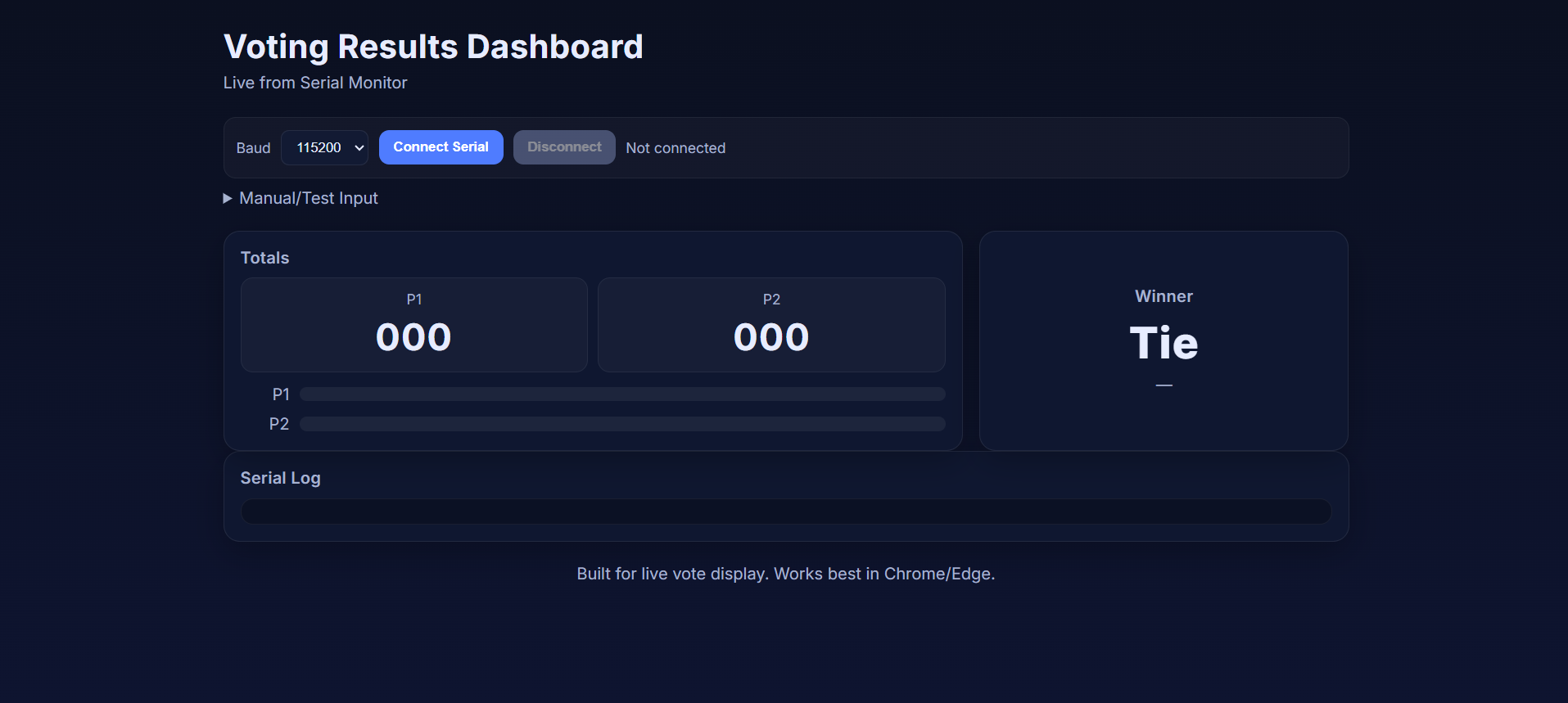
Electronic Voting Machine (FPGA)
2025 | Completed
A fully digital voting machine designed in Verilog on the iCEPi FPGA. The system simulates multiple voting inputs using switches and employs FSM logic to manage votes and counting. Results are sent over UART (9600 bps) to a Python + HTML interface for display.
Key Features:
- Multiple voting inputs using switches
- FSM logic for vote management and counting
- UART transmission at 9600 bps
- Python + HTML web dashboard for results display
Technical Implementation:
Technologies Used:
Digital Lock System (FPGA)
2025 | Completed
A Verilog-based digital lock system implemented on FPGA. The design uses buttons (btn1, btn2, encoder_btn) for input sequence, FSM for password verification. Lock/unlock status and attempts are transmitted via UART (9600 bps) to a Python + HTML web interface.
Key Features:
- Button inputs (btn1, btn2, encoder_btn) for password sequence
- FSM for password verification and lock logic
- UART transmission at 9600 bps
- Python + HTML web interface for monitoring